|
|
|||||||||
By Gunter R. Ladewig and Robert Lyn
Genrich Altshuller wondered, "Could inventions be the result of systematic inventive thinking?" Over half a century, Altshuller and his associates investigated hundreds of thousands of patents. They found that exceptional patents improved the performance of a technological system through elimination of its fundamental constraint by resolving contradictory requirements. Altshuller discovered that as technological systems evolved to their next level of performance by resolving contradictory requirements, systems tended to progress along certain vectors, or trends, of evolution. Each vector of evolution had discrete phases, or performance levels, which define where a system was, where it is and where it will be in its evolutionary journey. Another revelation was the frequent occurrence of a windfall of benefits, or super effects, which occurred when a system progressed from one phase to the next by eliminating its fundamental contradiction. Not only were many costly add-ons or processes, and expensive tolerances were no longer required, many systems had inherited valuable, new, product differentiating, capabilities and features. The result, the Theory of Inventive Problem Solving (TRIZ), provides a methodology for systematic creativity.
The increasing and never-ending demand for more function from electronic devices in smaller form factors continues to accelerate and force pressure upon electronics systems to meet these requirements. To satisfy these demands, designs must be optimized in order to remove the critical roadblocks to attaining maximum performance at minimal cost. An increasing amount of attention, which has traditionally been focused on semiconductor chip developments and systems design, is now being directed towards the most severe system performance constraint, i.e., the interconnection technologies used to join these components together. A new strategic interconnection technology, insulated wire bonding, is poised to remove the fundamental constraint that currently impedes the economic viability of next-generation, high performance designs. This paper describes the chain reaction of benefits, referred to by TRIZ as super effects, which occur when wire-bonding with with a micron-thin wire.
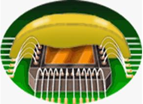
Wire bonding is the process of welding a fine conductive wire (usually gold), approximately half the diameter (25 microns) of a human's hair, from an integrated circuit (IC), chip interconnection pad to a substrate pad as shown in Figure 1. It is used in more than 90 percent of all IC packages.
Source: Loctite | |||||
Since total system performance is most severely limited by the length of chip-to-chip interconnecting wire as shown in Figure 2, requiring designers to minimize the number of chips used.
| |||||
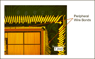
This constraint forces the designer into a trade-off contradiction: wires should be close, ideally touch to maximize input/outputs (I/O) per chip and the wires should be far apart to prevent electrical shorts. The wire bonding industry's answer to this dilemma was to space out wires by only bonding around the chip's perimeter as shown in Figure 3, resulting in decreased performance (low I/O per chip) and wasted expensive "real estate" at the center of the chip.
| |||||
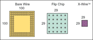
Because the industry never solved this fundamental issue, and due to the ever-increasing demand for more performance (I/O per chip), other – but very expensive – new technologies with area array capability such as an area array flip chip were developed. (See Figure 4.)
| |||||
Although flip chip provides some performance improvement, the unresolved interconnect wiring problem was never eliminated and merely transferred to expensive, multi-layer substrates with long layer-to-layer connecting conductors, as shown in Figure 5.
| |||||
As mentioned previously, Altshuller and his colleagues discovered that technological systems improve their performance, i.e., eliminate constraints, by evolving from one phase to the next, along predictable vectors of evolution. We can examine any technological system by determining which vectors are involved and what the system's maturity is, subject to the phase locations along various vectors. In other words, we can perform an innovation potential assessment on any system to determine its opportunities for improvement. We can determine if the system has room for improvement (more phases to exploit) with current technology, or if it is bumping its head at the end of a vector and for this reason must change to a new technology (new vector). We can also determine if an evolutionary phase has been skipped, enabling us to go back to that phase, exploit it and hollow-out the competition that has committed itself to a more expensive process and or infrastructure.
Subject to how the trends of evolution are grouped, there are more than 30 trends. The trend that applies to our most fundamental IC constraint, chip-to-chip interconnect wire length, chip wire-ability, is the trend of geometric evolution for a line. Generally speaking, geometric structures tend to evolve from a single point toward complex three dimensional structures as follows:
Point »» Line »» 2-D lines (planar) or curves »» 3-D Lines (cubic) or curves »» 3-D complex curves
Using sewing as an example, the first phase would be a single stitch, then a straight line of stitched thread, then a plane of woven or stitched fabric, next three dimensionally, interconnected layers of fabric, then three dimensionally interconnect complex structures.
Figures 1 to 3 reveal that phase 3, 2-D lines, in a planar arrangement was only partially completed. Because the contradiction of having wires touch to maximize the number of wires and at the same time have wires that are far apart to prevent electrical shorting was never solved, only peripheral chip bonding was used to maximize wire spacing, thus leaving the whole center of the chip completely empty. Or, if performance demands couldn't be satisfied by wire bonding, then expensive new technologies (like flip chip) were adopted.
This contradiction was solved by developing a one micron-thin, bond wire insulating material that has the ability to be used on standard wire bonding assembly equipment. With this technology the whole area of the chip, including its center, could now be wire bonded as seen in Figure 6, requiring fewer chips and resulting in improved total system performance due to fewer and shorter inter-chip wire connections.
| |||||
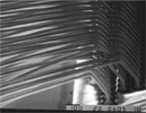
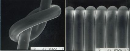
Numerous obstacles had to be overcome. To name a few, the coating 1) had to be thin, yet have high dielectric strength, 2) must have high flexural strength but crack resistant (see Figure 7), 3) must not inhibit bonding, 4) must be non-contaminating (leaving no residue on equipment), 4) be solvent resistant, 5) adhere to gold and 6) be temperature stable up to 250°.
| |||||
A chain reaction of super effects is poised to have a global impact on the electronics industry due to the implementation of this wire. To name a few, these are:
| |||||
A windfall of benefits were achieved in this situation when a technological system's fundamental constraint or contradiction was solved. Just one trend of evolution (out of more than thirty) can be used as a competitive weapon. Trends not only tell us where our products are on their evolutionary journey versus a competitor's product, for example, but also where products must evolve to. Perhaps most importantly, they show opportunities for improvement or, as in this case, how to hollow-out the competition when an evolutionary phase has been skipped.
TRIZ has many more applications and tools than what was shown in this example with the use of the trends of geometric evolution of a line. TRIZ provides a methodology, distilled from the real world of the worldwide patent base, for the creation of world-class products and processes that are based on the best tools used by the best inventors for the creation of their best ideas.
Gunter R. Ladewig is president of PRIMA Performance Ltd., a consulting company that specializes in product, process, and operational renaissance by applying TRIZ, TOC, the theory of constraints, Six Sigma and Lean manufacturing techniques. Gunter is an expert in operational efficiency improvement and world class product design. In 1992 he was winner of IBM’s Innovation Invitational, and in addition, twice on IBM’s winning team of the Government of Canada Award for Business Excellence: The Gold Award for Productivity, and the Gold Award for Quality. Most recently, Gunter is one of the authors of The PDMA, Product Development Management Association, TOOLBOOK 3 for New Product Development. Contact Gunter R. Ladewig at info (at) primaperformance.com or visit http://www.primaperformance.com/.
Robert Lyn is the chief technology officer of Microbonds Inc. Prior to Microbonds Inc., Robert spent more than 10 years with IBM Microelectronics and Celestica Inc. as a senior staff engineer in advanced packaging development. At IBM and Celestica, he led various teams which introduced a number of new microelectronics packaging technologies into the manufacturing process, including Chip-on-Board wire bonding technology, Flip Chip technology, Ball Grid Array chip carriers, Multi-chip modules and single chip packaging. These technologies have supported product offerings, such as PCMCIA Notebook cards, SIMM memory cards, RF/Wireless cards, Networking cards, Power Technology, PC motherboards, Workstations, Mainframe computers and Internet routing systems. Robert holds a BASc degree in Mechanical Engineering from the University of Toronto. Contact Robert Lyn at rlyn (at) microbonds.com or visit http://www.microbonds.com/.