|
|
|
|||||||||
|
|||||||||
By Mi Jeong Song, Vasily Lenyashin and Jeong Wook Lee
A light emitting diode (LED) is a semi-conductor device, which emits light by electrons moving from a point of high energy to a point of low energy when electric power is applied to it. LEDs are in widespread use – from cell phones to automobile lights. Increasing efficiency is one of biggest issues facing LEDs. There are several causes for decreasing light efficiency. One of the most serious sources of light loss lies with low extraction efficiency. Root cause analysis revealed that total internal reflection between a GaN/sapphire interface is the main source of low efficiency (harmful effect). By formulating technical contradictions around this issue, we suggest more than 30 fresh ideas, among which three were selected for feasibility test and prior art search. All three fresh ideas have increased light extraction efficiencies at a minimum of 40 percent. Two of the ideas were filed as patents, which were integrated into commercial LED chips successfully in October 2006. Other ideas (that were not accepted at that time) have been seed for further research and development milestones of the LED project team.
A light emitting diode (LED) is an illuminating semi-conductor diode device. In a diode system, current flows easily from the p-side (anode) to the n-side (cathode) but not in the reverse direction.1 Charge carriers – electrons and holes – flow and meet together in a p-n junction. When an electron meets a hole in the p-n junction, it falls to a lower energy level and releases energy in the form of light. The wavelength of the emitting light (color) depends on the band gap energy of the materials forming the p-n junction. The direct band gap of LED material determines the wavelengths of the emissions from near-infrared light to vis/near-ultraviolet light.
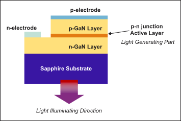
Since the mid-1990s, GaN has been of great interest because of its potential for optoelectronic application – for light emitting diodes, laser diodes (LD), LCD backlights, etc.2 Figure 1 shows the typical structure of an LED system – GaN, which comprises light emitting p-n junction (usually called the active layer), n-layer, p-layer, n-electrode, p-electrode and sapphire substrate.
| |||||
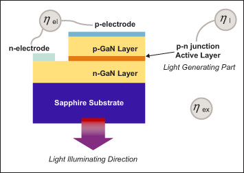
The light generating efficiency of an LED chip depends on three different efficiencies designated in the following formula:
hWPE = hi x hex x hel – where hWPE = wall plug efficiency of chip, hi = internal quantum efficiency, hex = extraction efficiency and hel = electrical efficiency
The internal efficiency is light generation efficiency that relies on semi-conducting material, dopant material, nano-structure of material (e.g., defects) and so on. Internal efficiency at the start was around 70 percent. Electrical efficiency has a close relationship with p-contact and n-contact. Increasing electrical efficiency was a priority, but the most serious problem was extraction efficiency at approximately 30 percent.
| |||||
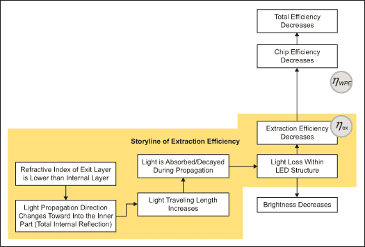
There have been many studies of LED light extraction efficiency issues.3,4,5,6 In the early stages of identifying harmful mechanism, LED domain experts suggested lots of probable reasons why LEDs had such poor extraction efficiency. With the use of TRIZ, the applied problem formulation technique helped construct the harmful mechanism in Figure 3.7
| |||||
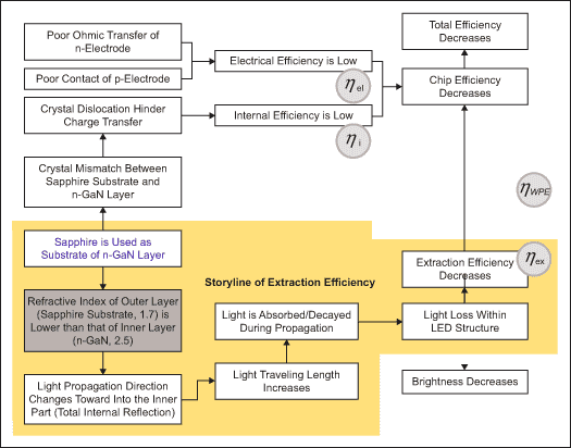
This causality diagram helped identify the "real" problem – showing the harmful effect chain from "sapphire is used as substrate of n-GaN layer" »» "refractive index of outer layer (sapphire substrate, 1.7, its nature of sapphire) is lower than that of inner layer (n-GaN, 2.5, also nature of GaN)" »» "light propagation direction changes toward into the inner part (total internal reflection)." After identifying the critical thread of root causes, it was necessary to understand the physical effects – total internal reflection – which had a main role in the harmful effect chain.
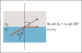
To understand the why and where of the problem, it was necessary to understand the nature of the total internal reflection phenomena more deeply. When light comes from a medium with a high refractive index to a medium with a lower refractive index, the light bends toward an interface direction (i.e., away from the normal direction). In this case, the exit angle from the normal direction is always bigger than the incident angle of the light. As the incident angle becomes larger, the exit angle approaches 90°. For some angles greater than the critical incident angle øc, the light cannot go out from the first media – the light is kept in the first media. There is a risk of such total internal reflection where two types of media meet, which have different refractive indices. In LED, the incident lights a perpendicular pathway from the substrate/LED inter-facial layer.
| |||||
Total internal reflection explains why LEDs had low extraction efficiency. It was necessary to create a system to eliminate the harmful effect of the total internal reflection mechanism. To design the system, the resources were more deeply examined, especially the operating zone in the LED. The refractive index vs. device location showed where there may be the most serious total internal reflection. (Figure 5 shows the specific location and Table 1 describes the location.)
| |||||
| Table 1: Resource Analysis for the Location of Total Internal Reflection | |||||
| Inner Part | N_in (Inner Part) | Outer Part | N_out (Outer Part) | Dn (In-Out) | Severity of Total Internal Reflection |
| InGaN Quantum Well | 3.00 | N-GaN | 2.54 | 0.46 | Medium |
| N-GaN and Buffer Layer | 2.54 | Substrate (sapphire) | 1.46 | 1.12 | High |
| Substrate | 1.78 | Epoxy | 1.50 | 0.28 | Low |
| Epoxy | 1.50 | Air | 1.00 | 0.50 | Medium |
After analyzing the harmful relationship between sapphire substrate and GaN substrate, questions focused on why the sapphire existed with such a harmful effect. The answer? Without sapphire substrate, GaN itself cannot be formed. The GaN crystal can grow only on crystal substrate with a similar crystal structure. The idea formed of using the GaN itself as a substrate with the same refractive index, but such substrate is more expensive than the sapphire substrate.
The causality diagram of the light extraction efficiency problem needed updating because the old version had no information about the function of sapphire substrate. In Figure 5, the yellow background area was the region of focus for extraction efficiency. Supplemental information had meaningful links with one of the root causes for extraction efficiency. Figure 6 shows the more realistic problem model of light extraction efficiency (opposed to the version shown in Figure 3). This illuminated the core of the problem – there existed an inherent contradiction relationship.
| |||||
Often, it is necessary for a TRIZ practitioner to work with domain experts to extract and understand the problem of the system. The TRIZ specialist must guide domain experts to externalize core problems of the system correctly, not because TRIZ is not useful, but because TRIZ itself cannot understand a problem's structure.
After coming to a consensus on the root cause of the system, it is time to suggest a primary solution to eliminate the problem – the transition action.8 The most interesting feature of a known solution is a method of changing interface geometry to change a critical angle of total internal reflection. This transition action solves identified root causes to understand where to go, i.e., to set up a problem solving strategy.
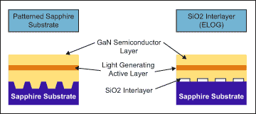
The ELOG (epitaxial lateral overgrowth, seen right in Figure 6) technique and PSS (patterned sapphire substrate, left in Figure 6) technique were useful for reducing the total internal reflection between sapphire substrate and GaN.9,10,11 The original purpose of these two techniques was to reduce dislocation density during crystal epitaxial growth. The primary effect of these two techniques is increasing the internal quantum efficiency by reducing defects of the crystal. The enhancement of light extraction efficiency is a secondary effect of the suggested technologies.
But these techniques had inherent problems. ELOG needs the introduction of an additional SiO2 mask layer on the sapphire substrate, which enhances manufacturing complexity. PSS is a more advanced technique than ELOG because an additional mask is not necessary. But the conventional PSS process has poor manufacturing efficiency. When growing the semi-conductor crystal layer on the conventionally patterned sapphire substrate, a planarization process (creation of an even surface) was necessary after facet growth occurred on the pattern. The facet grows on the top and bottom parts of the pattern; crystal re-grows to planar surface – a thick layer is necessary. Another disadvantage of the conventional PSS technique is void formation on the interface of sapphire substrate and GaN. Lateral growth speed is faster than vertical growth speed in GaN semiconductor epitaxial growth. Rapid lateral growth on the conventional groove pattern leads to void formation.
To formulate a problem model, it is necessary to summarize the collected information. The beginning of the project started with the undesirable feature of the LED system. Figure 7 shows several descriptions about the cause of the problem, the known way to resolve said problem, and the problem of the known method – in other words, showing why using known ways is not an ideal solution.8
| |||||
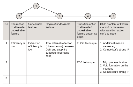
Figure 7 shows the knowledge of the undesirable function (point 1), the reason to eliminate the undesirable function (point 2), and the cause of the undesirable function (point 3). Point 4 is the starting point of active analysis – where transition action was used to work on the identified and undesirable feature of the problem's origin. At point 5, analyses of drawbacks of such transition actions and/or why the known transition action to eliminate undesirable function could not be used. Figure 7 not only summarizes the problem formulation, but also provides a template for problem model formulation.
A technical contradiction could be defined at any hierarchy in a system/problem complex denoted in a root cause analysis diagram. For the purpose of product design upgrade, a competitor's solution for the same problem is a pragmatic starting point of the contradiction resolution journey. The pragmatic contradiction is defined as follows:
TC 1-0: If the SiO2 mask is introduced on the sapphire substrate (via the ELOG technique), the total internal reflection is reduced (good), but the additional mask generates manufacturing complexity (bad).
TC 1-1: If the SiO2 mask is absent (conventional even structure), the manufacturing complexity is minimized (good), but total internal reflection exists (bad).TC 2-0: If a groove pattern is introduced on the sapphire substrate (via the PSS technique), total internal reflection is reduced (good), but the manufacturing process is slow (bad 1) and avoid appears on the interface (bad 2).
TC 2-1: If a groove pattern is absent (conventional even structure), manufacturing complexity is minimized (good), but total internal reflection exists (bad).
According to the domain experts, introducing a mask during manufacturing process is complex, which increases the cost of the device; therefore the decision was made to follow groove introduction (TC 2-0) – because efficiency enhancing met the requirements of customers.
The contradiction: introduction of groove to reduce total internal reflection (good) «» manufacturing process time (bad) and unwanted void on the interface (bad). Using the contradiction matrix led to the generation of relevant parameters illuminating: shape «» object generated harmful factors, shape «» object affected harmful factors. (See Table 2.)
| Table 2: Contradiction Matrix Use Results | |||
| Worsening Feature | Object Generated Harmful Factors | Object Affected Harmful Factors | |
| Improving Feature | Shape | Parameter change, 35 | Blessing in disguise, 22 Segmentation, 1 Separation, 2 Parameter change, 35 |
Of the recommended principles, parameter change (35) seemed the most promising direction for further ideation. The controllable parameters in the system follow:
The parameters of the shape of the groove could be changed in a number of ways – the pitch, width, height, shape, refractive index difference, distribution of pitch, width, height, shape, refractive index difference, etc. Curvature (principle 14) also suggested changing the pattern.12
Once deciding to change the shape of the groove to curve shape, the benefits of such variations were estimated. A GaN semi-conductor crystal grows in a specific direction. Crystal growth on such a curved shape is restricted by GaN epitaxial growth. Ray tracing (by code V optical stimulator) was tried to simulate the effectiveness of the curved shape on total internal reflection. According to the positive results proven by the ray tracing simulator, structure designs were selected for manufacturing process design.
The problem was the lack of a method to develop the curved pattern on the substrate. By using a lithography technique, domain experts created the curved shape of sapphire substrate. Upon the curve-patterned sapphire substrate, GaN crystal growth proceeded more rapidly than that of the conventional groove pattern.13
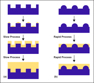
Figure 8 summarizes the different mechanisms of GaN epitaxial crystal growth on two different patterns. Facet formation – the growing conventional patterned substrates increases process time of crystal growth, which then worsens productivity. The circular shape of the sapphire pattern never grows crystal on it, which thus accelerates crystal growth more rapidly.14
| |||||
The curved pattern showed excellent light extraction efficiency with minimal irritation in manufacturing process – without avoiding known technologies in patents. Curve-shape sapphire substrate is one of the key technologies introduced in LED lamps.15
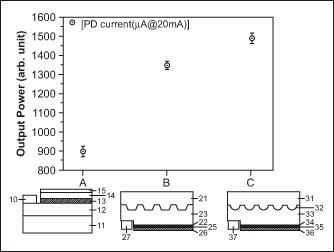
A: conventional, B: competitor's design, C: proprietary design | |||||
Figures 8 and 9 show the differences of performance between the conventional device (A), the simple corrugation structure of sapphire (B) and the curved corrugation structure of sapphire (C). The light extraction efficiency of case B (in which the light-emitting device is formed on the simple corrugated substrate) is 50 percent greater than case A (in which the light-emitting device is formed on the even substrate). The light extraction in case C – with the ideas generated by TRIZ activity (in which the light-emitting device is formed on the curved substrate) – extracts light 60 percent more than in case A. In addition, the light extraction in case C is approximately 10 percent better than case B, because C's circular corrugation plays the role of an optical lens that changes the light path and at the same time reduces the defect density of the growing semiconductor crystal layer. Although similar concepts had been tried before, the curve patterned substrated was patented and has proven successful.16,17,18,19,20
One of the critical problems in a conventional GaN LED system was analyzed using the TRIZ methodology. After resource analysis, the total internal reflection between GaN and sapphire substrate was recognized as most serious source of the low extraction efficiency problem. Known solutions (i.e., transition action for the total internal reflection) were critically surveyed in a problem formulation table. Contradictions caused by transition actions were formulated and resolved with the guidance of inventive principles that suggested conceptual guidelines for technical contradiction. More than 20 useful ideas were developed with the aid of the inventive principles. Many ideas have proven excellent performers for light extraction – up to a 60 percent increase. Two ideas were filed up as U.S. patents and served as an important technology for real LED chip production.
This project was executed from May-September 2003. More than 25 technical ideas were suggested; two were filed as international patents. One concept created by this project was introduced in a real LED system produced by Samsung Electromechanics, Inc. With the aid of TRIZ, the "light extraction efficiency of LED is low" problem was understood more thoroughly and the solutions for the problem more easily developed. The LED division of Samsung Electromechanics then released brighter LED-based backlight units for cell phones in 2006.16
At the end of the process, the TRIZ practitioners forecasted the near future of the LED system. According to the pattern of an increasing segmentation level, the light extraction structure will become smaller until reaching nano-level. Current papers and patents are looking at nano-structure in many areas. The rapid realization of the suggested ideas was aided by statistical assistance of Six Sigma.
Special thanks to Dr. Yoon, Suk Ho, Dr. Kim, Hyun Soo, Mr. Cho, Je Hee, Dr. Son and Chul Soo for their enthusiastic supports of TRIZ, idea development and realization. Special thanks to Mr. Cheong, Se Ho and all current and former members of the Six Sigma research group in SAIT.
Mi Jeong Song is a TRIZ consultant, She received her Ph.D. in chemical enginering at KAIST (Korea Advanced Institute of Science and Technology), Taejeon, Korea in 2000. She joined SAIT (Samsung Advanced Institute of Technology) upon graduation and spent her first two years in DNA chip development as a field engineer. In 2002, she joined their research innovation team. Dr. Song worked to customize conventional TRIZ with Six Sigma and SAIT MOT (management of technology) processes. She teaches TRIZ and consults on SAIT R&D topics. Mi Jeong Song has 23 U.S. patents as a result of her TRIZ consulting and is developing a pratical process of technology prediction for SAIT. Contact Mi Jeong Song at mijeong.song (at) samsung.com.
Vasily Lenyashin was born in 1946 in Russia. His background is as an engineer of electronic technique. He has more then 30 years experience in semi-conductor devices manufacturing. Mr. Lenyashin is author/co-author of more than 20 patents. Beginning in 1999, he has been a TRIZ advisor to Samsung, South Korea. Contact Vasily Lenyashin at vassili (at) samsung.com.
Jeong Wook Lee received his Ph.D. in materials science and engineering in 2002 from Sungkyunkwan University, Suwon, Korea. From 2002 to 2007, he was with the Samsung Advanced Institute of Technology (also in Korea) as a member of the senior research and development staff. Dr. Lee is working on the epitaxial growth of III-Nitride semi-conductor and light-emitting devices as a senior engineer of Samsung Electro-Mechanics Co. Ltd. Contact Jeong Wook Lee at jwlee115 (at) samsung.com.